
Author Affiliations
Abstract
1 Shenzhen Key Laboratory of Ultraintense Laser and Advanced Material Technology, Center for Advanced Material Diagnostic Technology, and College of Engineering Physics, Shenzhen Technology University, Shenzhen 518118, China
2 School of Physics, State Key Laboratory of Crystal Materials, Shandong University, Jinan 250100, China
With different interactions between material and femtosecond lasers, two-dimensional (2D) and three-dimensional (3D) waveguide couplers, whose separation distances are fabricated in z-cut lithium niobate crystal by femtosecond laser writing, are reported. Experimentally and numerically, it is shown from results that the guidance is only propagating along TM polarization due to the Type I modification and holds equal splitting ratios, which are the same as power splitters at 632.8 nm. The propagation losses of 2D and 3D waveguide couplers exhibit better transmission properties than those of the previously reported Type I Y-junction waveguide splitters.
femtosecond laser writing beam splitters lithium niobate Chinese Optics Letters
2023, 21(11): 112201
Author Affiliations
Abstract
1 State Key Laboratory of Advanced Optical Communication Systems and Networks, University of Michigan-Shanghai Jiao Tong University Joint Institute, Shanghai Jiao Tong University, 200240 Shanghai, China
2 State Key Laboratory of High Field Laser Physics, Shanghai Institute of Optics and Fine Mechanics (SIOM), CAS Center for Excellence in Ultra-Intense Laser Science, Chinese Academy of Sciences (CAS), 201800 Shanghai, China
3 Department of Physics and Astronomy, Shanghai Jiao Tong University, 200240 Shanghai, China
4 School of Physics and Electronic Science, East China Normal University, 200241 Shanghai, China
5 Department of Physics and Astronomy, College of Staten Island, the City University of New York, 10314 New York, USA
Transparency and perfect absorption are two contradictory terms; a perfect absorber never permits waves to transmit through. However, this statement only remains true in the linear regime, where the nonlinearity has been omitted and the physical system like the perfect absorber is not affected by the incoming waves. Here we experimentally demonstrate an intriguing self-induced transparency effect in a perfectly absorbing optical microcavity, which perfectly absorbs any incoming waves at the low power level, but allows a portion of waves to be transmitted at the higher power due to the nonlinear coupling between the fundamental and its second harmonic modes. Moreover, the asymmetric scattering nature of the microcavity enables a chiral and unidirectional reflection in one of the input ports, this leads to asymmetric and chiral coherent control of the perfect absorption states through phase varying. More importantly, such chiral behaviors also empower the chiral emission of second-harmonic generation with a high distinct ratio in the transparency state. These results pave the way for controllable transparency in a wide range of fields in optics, microwaves, acoustics, mechanics, and matter waves.

Author Affiliations
Abstract
1 Centre de Nanosciences et de Nanotechnologies, CNRS, Université Paris-Sud, Université Paris-Saclay, 91120 Palaiseau, France
2 Université Côte d’Azur, Institut de Physique de Nice, CNRS-UMR 7010, Sophia Antipolis, France
3 Department of Physics and Astronomy, College of Staten Island, CUNY, Staten Island, New York 10314, USA
4 Graduate Center, CUNY, New York, New York 10016, USA
5 Université de Paris, 75205 Paris Cedex 13, France
Zero modes are symmetry protected ones whose energy eigenvalues have zero real parts. In Hermitian arrays, they arise as a consequence of the sublattice symmetry, implying that they are dark modes. In non-Hermitian systems that naturally emerge in gain/loss optical cavities, particle-hole symmetry prevails instead; the resulting zero modes are no longer dark but feature phase jumps between adjacent cavities. Here, we report on the direct observation of zero modes in a non-Hermitian three coupled photonic crystal nanocavities array containing quantum wells. Unlike the Hermitian counterparts, the observation of non-Hermitian zero modes upon single pump spot illumination requires vanishing sublattice detuning, and they can be identified through far-field imaging and spectral filtering of the photoluminescence at selected pump locations. We explain the zero-mode coalescence as a parity-time phase transition for small coupling. These zero modes are robust against coupling disorder and can be used for laser mode engineering and photonic computing.
Photonics Research
2022, 10(2): 02000574
Author Affiliations
Abstract
Shanghai Institute of Space Power-sources, Shanghai 200245, China
Multijunction solar cells are the highest efficiency photovoltaic devices yet demonstrated for both space and terrestrial applications. In recent years five-junction cells based on the direct semiconductor bonding technique (SBT), demonstrates space efficiencies >35% and presents application potentials. In this paper, the major challenges for fabricating SBT 5J cells and their appropriate strategies involving structure tunning, band engineering and material tailoring are stated, and 4-cm 2 35.4% (AM0, one sun) 5J SBT cells are presented. Further efforts on detailed optical managements are required to improve the current generating and matching in subcells, to achieve efficiencies 36%–37%, or above.
Journal of Semiconductors
2021, 42(12): 122701
1 中国科学院上海技术物理研究所,红外物理国家重点实验室,上海 200083
2 上海空间电源研究所,空间电源技术国家重点实验室,上海 200245
3 中国科学院大学,北京 100049
现有1.0 eV/0.75 eV InGaAsP/InGaAs双结太阳电池的开路电压小于各子电池的开路电压之和,鲜有研究探索开路电压损耗的来源以及如何抑制。通过研究发现,InGaAs底电池背场/基区界面处的少数载流子输运的主要机制是热离子发射,而不是缺陷诱导复合。SIMS测试表明,采用InP或InAlAs背场均不能有效抑制Zn掺杂剂的扩散。此外,由于生长过程中持续的高温热处理,III-V族主元素在界面处发生了热扩散。为了抑制上述现象,提出了一种新型InP/InAlAs超晶格背场,并应用到InGaAs底电池中。制备得到的双结太阳电池在维持短路电流密度不变的情况下,开路电压提升到997.5 mV,与传统采用InP背场的双结太阳电池相比,开路电压损耗降低了30 mV。该研究成果对提升四结太阳电池的整体开路电压有重要意义。
背场 InGaAsP/InGaAs双结电池 开路电压 超晶格 Back-surface field InGaAsP/InGaAs dual-junction open-circuit voltage superlattice
1 中国科学院 上海技术物理研究所, 上海 200048
2 上海空间电源研究所, 上海 200245
3 中国科学院大学, 北京 100049
Ⅲ-Ⅴ族太阳电池效率的持续提升要求对能量转换材料的带隙宽度进行更细致划分, 以实现对全光谱的高效利用。在短波红外波段, 四元InGaAsP混晶材料因在带隙宽度和晶格常数的调节上具有很好的可操作性, 是一种极具潜力的短波红外光电转换材料。本文对InGaAsP材料生长及子电池器件制备进行了研究, 通过时间分辨荧光光谱、高分辨X射线衍射等表征手段对室温下晶格失配的InGaAsP材料进行了测试分析。实验结果表明, 在一定程度负失配生长条件下, InGaAsP材料质量随着负失配程度逐渐提高。在后续电池制备过程中, 一定程度负失配同样有助于电池器件性能提升, 制备的单结电池开路电压由晶格匹配时的633 mV提高到负失配条件下的684 mV, 从而为高效多结太阳电池的应用提供了新的技术路线。
晶格失配 太阳电池 lattice-mismatch InGaAsP InGaAsP MOCVD MOCVD solar cell
农业农村部植物营养与肥料重点实验室, 中国农业科学院农业资源与农业区划研究所, 北京 100081
为了明确不同生育时期进行玉米氮素营养诊断的叶片层位, 建立准确稳健的玉米氮素营养诊断模型, 以达到合理追施氮肥, 提高氮肥利用率的目的。 试验采用单因素盆栽试验设计, 以玉米(郑单958)为研究对象, 应用高光谱技术, 分析了不同氮营养水平下不同生育时期不同层位玉米叶片的氮含量分布和变化规律及光谱响应特征; 并依据叶片氮含量与光谱反射率的相关关系, 叶片氮含量与全波段(400~2 000 nm)任意两两波段组合构建的比值光谱指数(RSI)的回归关系, 初步确定了不同生育时期进行氮素营养高光谱诊断的目标叶片, 筛选出最优的比值光谱指数, 建立了叶片氮素含量估算模型。 结果表明: 玉米叶片氮含量: 上层>中层>下层; 随着玉米的生长, 在低氮条件下上层叶片氮含量呈先减少后增加(追肥)再减少趋势, 在高氮条件下呈减少趋势, 中下层叶片氮含量呈递减趋势。 六叶期下层玉米叶片光谱反射率敏感范围较大, 相关性较强; 九叶期和灌浆期上层玉米叶片的光谱反射率敏感范围较广, 相关性较强; 开花吐丝期中层叶片的光谱反射率敏感范围较大, 相关性较强。 六叶期选取下层叶作为诊断目标叶, 选取最佳比值光谱指数RSI(1 811, 1 842)建立线性估算模型, 九叶期和灌浆期选取上层叶片作为诊断目标叶, 选取的最佳比值光谱指数分别为RSI(720, 557), RSI(600, 511)建立线性估算模型, 开花吐丝期选取中层叶片作为诊断目标叶, 选取比值光谱指数RSI(688, 644)建立线性估算模型。 研究结果可为快速准确地利用光谱技术进行玉米叶片氮素营养诊断提供理论依据。
玉米叶片 氮素含量 光谱指数 分层诊断 Maize leaf Nitrogen Content Spectral index Diagnosis layer 光谱学与光谱分析
2019, 39(9): 2829
1 西安邮电大学 电子工程学院, 陕西 西安 710121
2 西安邮电大学 理学院, 陕西 西安 710121
采用COMSOL有限元分析软件的固体传热模块, 对有机电致发光器件(OLED)的热学特性进行了仿真, 发现器件温度随着输入功率成线性增大。在驱动电流为150 mA·cm-2时, 仿真结果表明, Alq3发光层的最高温度为82.994 3 ℃; 玻璃基板下表面的最高温是77.392 6 ℃; 器件阴极表面中心区域的最高温度为82.994 2 ℃, 其平均温度为78.445 ℃。通过改变功能层热传导率、功能层厚度、对流换热系数、表面发射率等参数模拟其对OLED器件热学特性的影响, 结果表明, 当增加基板的热传导率时, OLED器件温度显著下降而且表面及内部温度梯度大幅减小; 提高空气对流换热系数及基板的表面发射率, OLED的温度可以大幅减小。而其他参数则对其影响并不明显。
有机电致发光器件 有限元分析 温度分布 热学特性 散热 organic light emitting device finite element analysis temperature distribution thermal characteristics thermal dissipation 红外与激光工程
2018, 47(7): 0720001
Author Affiliations
Abstract
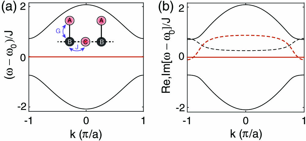
1 Department of Engineering Science and Physics, College of Staten Island, CUNY, Staten Island, New York 10314, USA
2 The Graduate Center, CUNY, New York, New York 10016, USA (li.ge@csi.cuny.edu)
In this work, we first discuss systematically three general approaches to construct a non-Hermitian flat band, defined by its dispersionless real part. These approaches resort to, respectively, spontaneous restoration of non-Hermitian particle-hole symmetry, a persisting flat band from the underlying Hermitian system, and a compact Wannier function that is an eigenstate of the entire system. For the last approach in particular, we show the simplest lattice structure where it can be applied, and we further identify a special case of such a flat band where every point in the Brillouin zone is an exceptional point of order 3. A localized excitation in this “EP3 flat band” can display either a conserved power, quadratic power increase, or even quartic power increase, depending on whether the localized eigenstate or one of the two generalized eigenvectors is initially excited. Nevertheless, the asymptotic wave function in the long time limit is always given by the eigenstate, in this case, the compact Wannier function or its superposition in two or more unit cells.
Guided waves Waveguides Systems with special symmetry Photonic bandgap materials Photonics Research
2018, 6(4): 04000A10


